
 Through the partnership with Uber, we will harness Hyundai’s businesses and technologies to deliver true freedom of mobility.

long time ago in a galaxy far, far away,” there were airspeeders. The repulsorlift vehicles—featured in the iconic Star Wars franchise created by George Lucas—used skylanes to move in and out of dense traffic and maneuver between towering buildings on urban planets like Coruscant.
The idea of people traveling highways in the sky is no longer fodder for science fiction and fantasy. On Jan. 6, 2020 Uber and Hyundai Motor Co. announced a new partnership to develop Uber air taxis for a future aerial ride share network at the Consumer Electronics Show (CES) 2020 in Las Vegas. As part of the media event, Hyundai unveiled its S-A1 prototype. The automaker will produce and deploy the all-electric personal air vehicles (PAV), and Uber will provide airspace support services, connections to ground transportation and a ridesharing app called uberAIR.
Eric Allison, head of Uber Elevate, told CES attendees, “Hyundai is our first vehicle partner with experience in manufacturing passenger cars on a global scale. We believe Hyundai has the potential to build Uber air vehicles at rates unseen in the current aerospace industry, producing high-quality, reliable aircraft at high volumes to drive down passenger costs per trip.”
According to a new market research report, the market space for urban air mobility is projected to grow to $15.2 billion by 2030.
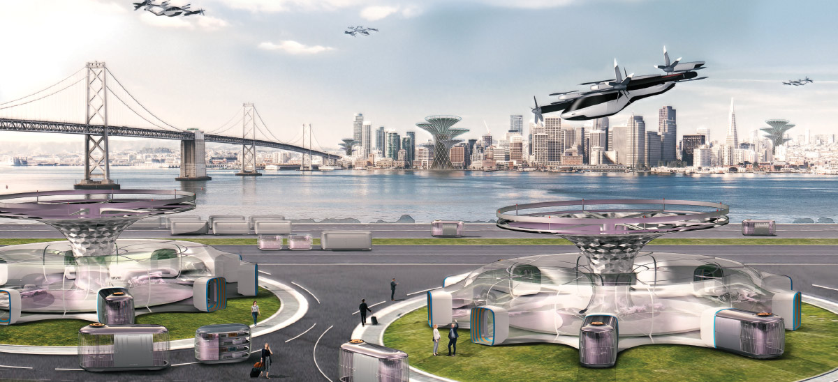
“Our vision of Urban Air Mobility (UAM) will transform the concept of urban transportation,” said Jaiwon Shin, executive vice president who leads Hyundai’s Urban Air Mobility division. “We expect UAM to vitalize urban communities, liberate people from gridlock and reclaim time for people to reinvest in activities they care about and enjoy.”
The carmaker engineered its concept for the S-A1 in part through Uber’s open design process, which mimics NASA’s practice of releasing design concepts to the public to spark innovation and incite research and investigation into such functions as wing design, noise, aerodynamics and simulation verification.
The S-A1—which employs electric vertical takeoff and landing (eVTOL) technology—is designed to take off vertically, convert to wing-borne lift in cruise and then revert to vertical flight for landing. It can hold up to four passengers and a pilot but Hyundai says the S-A1 will eventually become autonomous.
The PAV uses distributed electric propulsion to power multiple rotors and propellers installed around the airframe. The redundant system enhances safety and reduces noise. The S-A1 can cruise at up to 180 mph, attain a cruising altitude of 1,000 to 2,000 ft. and fly single trips up to 60 miles. Recharging the PAV during peak hours of operation is expected to take just five to seven minutes.
Uber estimates that commuters may be able to book an Uber air taxi as early as 2023 but among the hurdles it must overcome are standardization, certification, air traffic control, automating the pilot function and insurance liability. UberAIR also needs things like the vehicles themselves, skyports and batteries.
“Whether we are talking about air taxis, the electric vehicle market or the latest internal combustion engine car models, it all boils down to connectivity,” says Ken Kaufmann Jr., president of CEP Technologies Corp. “How fast we can communicate and how much data we can transfer to and from the vehicle in a short period of time.”
Printed circuit boards (PCB) are the brains that provide electricity and connectivity between the components of everything from smartwatches, phones and cell towers to vehicle GPS systems 0equipment aboard aircraft. Demand for PCBs—and the precision stamped parts needed to build them— is growing. Research and Markets estimates the value of the global PCB market will reach $89.7 billion by 2024.
 Whether we are talking about air taxis, EVs or the latest internal combustion-engine car models, it all boils down to connectivity.
“The number of PCB boards being installed on cars bumper to bumper is pretty mind blowing,” Kaufmann says. “They control all facets of a driver’s experience from entertainment and navigation systems to warning sensors and features like autonomous parallel parking.” In order for these things to function without interruption, he says, “you have to protect the PCB boards and what is on them with a shielding frame and cover that is mounted around these components to encapsulate them.”
The company produces shielding components that suppress and prevent internally generated signals and external ambient temperatures from interfering with equipment operations. Its two-piece covers and frames protect a variety of PCB board components. Parts are produced from alloys such as copper-nickel-silver (bare and preplated with tin), cold-rolled steel and 300 series stainless in precision coil thicknesses ranging from 0.004 in. to 0.015 in.
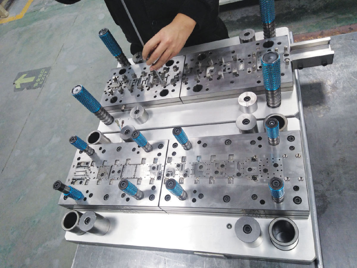
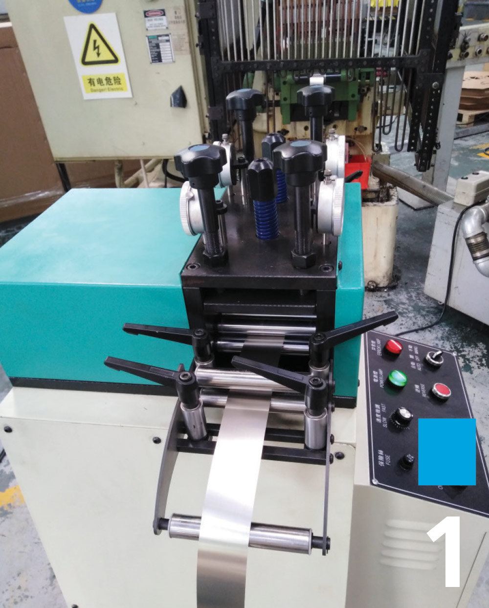
Parts are run on high-speed, straight-side stamping presses.“Tonnage isn’t a factor,” says Kaufmann, “it’s a matter of part complexity. If we are making a simple shield, we can make that part on a 15-ton to 20-ton press. For parts with complex features, we have to design and build longer dies to accommodate multiple forming operations. That calls for a longer bed length [and higher tonnage].”
Part feature and dimensional tolerances are critical, requiring numerous, meticulous profile cuts. In addition to ensuring that cuts and geometries are exact, part flatness is ultra-critical, as these frames are then soldered to a PCB board and sealed. CEP maintains a profile tolerance of 0.0015 in., a maximum part burr size of 0.0005 in. and flatness tolerances of less than 0.003 in.
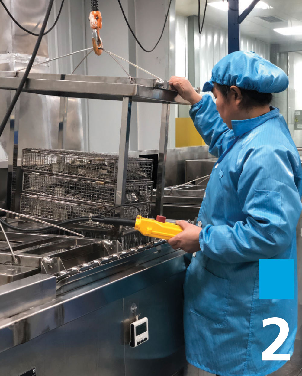
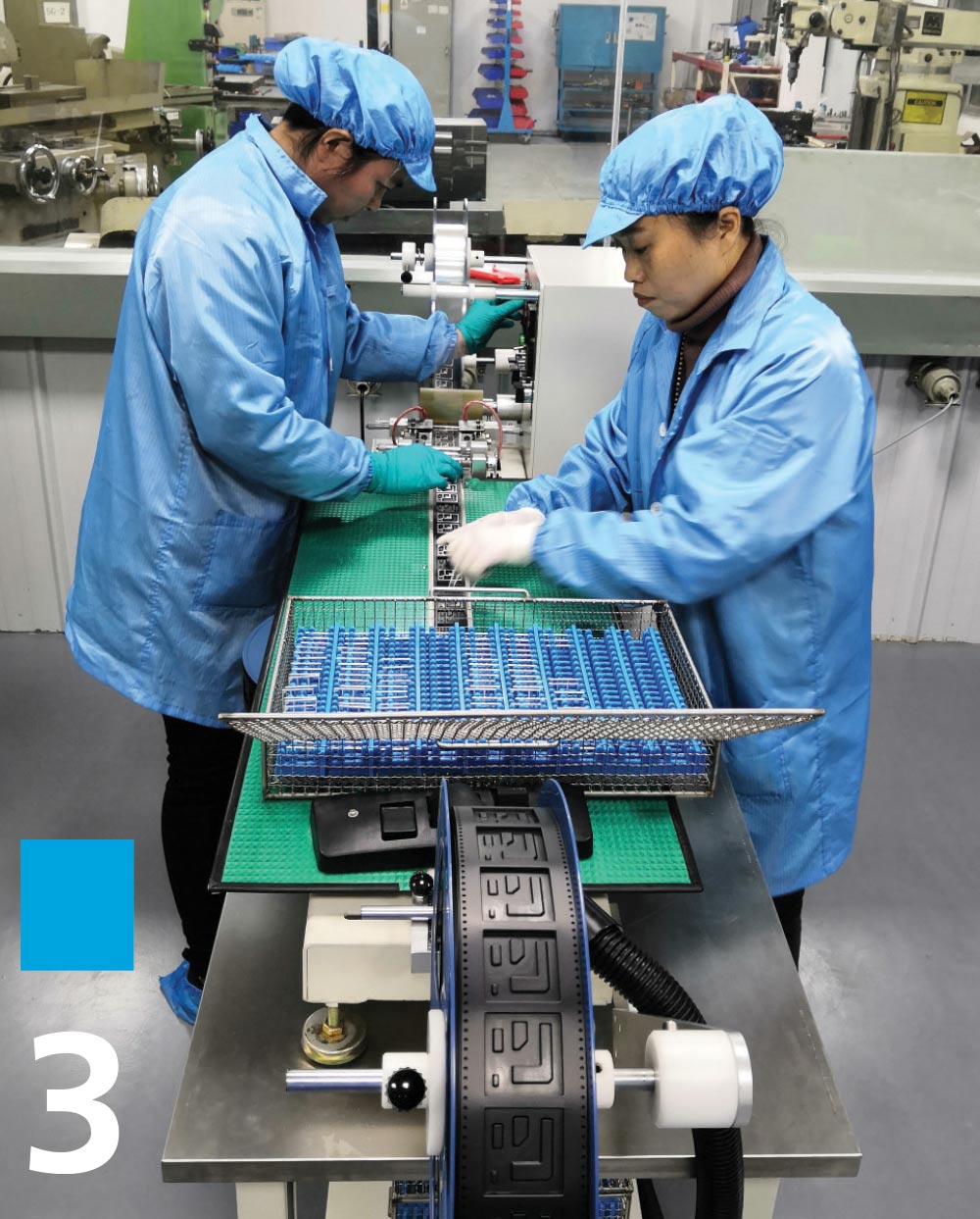
2. CEP’s technical cleaning methods meet ISO 16232 standards.
3. CEP’s tape and reel process protects parts dimensionally and strict technical cleanliness levels.
“It used to be that prints for parts contained a general note that mentioned cleanliness,” says Kaufmann. “Over the last five years, technical cleanliness requirements are at the heart of both the stamping and automotive industries.”
Technical cleanliness refers to determining the maximum particle size for metallic and non-metallic particles as well as the number of particles for each particle size metallic and non-metallic. Each application, feature or section of a car may have its own set of specifications.
“A fuel pump may have cleanliness standards that are different from that of an electronic door locking system,” Kaufmann explains. “Once you get to EMI/RFI shielding, you reach one of the most stringent levels of cleanliness in a vehicle.
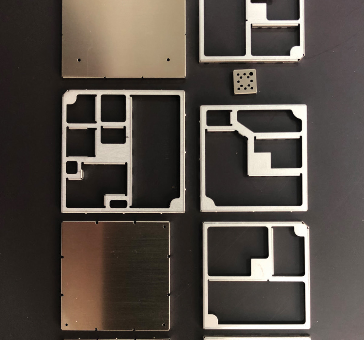
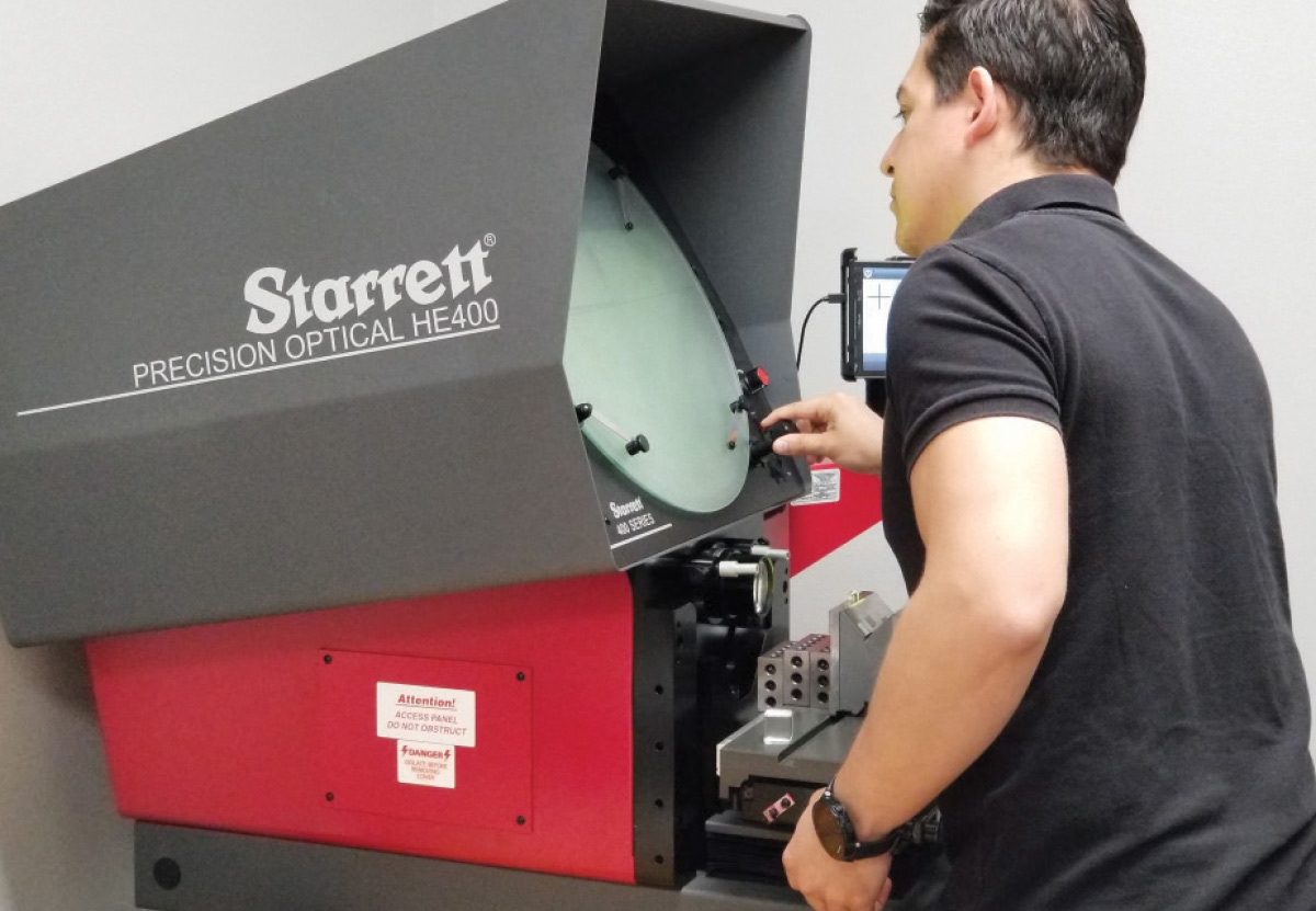
Current automotive specifications require CEP to hold particle sizes to less than 200µm but Kaufmann expects that to change with the introduction of 5G (the fifth generation wireless technology for digital cellular networks), which promises a wireless wide area network (WAN) with the ability to provide 24/7 connectivity for people, places and things.
“We’re working towards 100µm maximum particle size with the ultimate goal of 50µm for automotive requirements,” he says. To keep pace with customer expectations, CEP has continued to broaden its knowledge base around metal stamping and around value-added tangential tasks like technical cleanliness.
“This is where you make your biggest improvements in technical cleanliness standards,” Kaufmann says. “In order to achieve tighter and tighter technical cleanliness requirements, the total process needs to be controlled—from tooling, feeding material into the die and part ejection to part-on-part contact after the stamping process. Even your environment can be a culprit.”
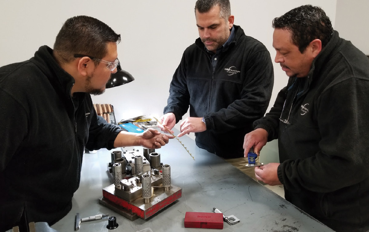
Until now, the stamper’s cleaning and packaging operations were housed in China. This year, CEP will expand its cleaning and tape-and-reel operations to San Antonio to support the EMI/RFI market in the United States and Mexico.
“Tape and reel is a value-added service that aids automated assembly,” Kaufmann explains. “It allows each part to be oriented in a specified manner and it provides a high level of protection to the part dimensionally and in terms of cleanliness.”
With Hyundai and Uber joining forces to launch a fleet of flying taxis, metalformers may need to take action to keep up. CEP, as a multifaceted, engineering-based stamper, offers one possible model. “Technology isn’t going to slow down,” Kaufmann says. “You have to adapt to marketplace changes by making sure your company is providing the value-added services your customers need.”